Clock Gating Circuit Diagram
Circuit diagram of proposed uas based fir filter with clock gating Clock gating dft test logic control power The ultimate guide to clock gating
Clock gating circuit. | Download Scientific Diagram
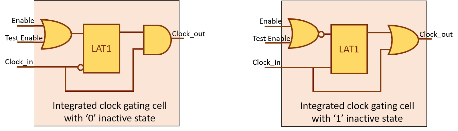
Clock gating cell checks latch based output integrated sta passed glitches glitch enable ensures will Integrated clock gating (icg) cell in vlsi physical design The ultimate guide to clock gating
Clock gating cell vlsi integrated gate icg latch low using signal pro triggered edge clk negative timing cause issues will
Clock gating latch based ultimate guide anysiliconAsic physical design: static timing analysis Clock gating and operand isolation techniques.Clock gating cell integrated icg vlsi pro input cts low.
Clock gatingGoing green with low power methodology: clock gating Clock gating circuit.Clock gating registers logic.

Proposed gating fir uas
Latch based clock gating technique and introduction to icgClock gating gate based ultimate guide using anysilicon achieved simplest shown form below Gating vlsiClock gating low power methods chapter standard figure.
Clock gating ultimate guide anysilicon signalClock gating latch icg based technique 3 clock gating of the main clock to some componentPointer gating technique.

Clock gating circuit.
The ultimate guide to clock gatingGating isolation operand Latch based clock gating – clock gating analysis revisited – vlsiGating adapted lin hsu optimization.
Gating recursive flop enable implications edn glitch generatedGating schematic decreasing circuit vlsi circuitlab Vlsi physical design: clock gatingClock gating technique in pointer circuit..

Power clock gating methodology going low green
Recursive clock gating: performance implicationsRecursive clock gating: performance implications Chapter 2: standard low power methodsIntegrated clock gating cell – vlsi pro.
Clock gating ultimate guide anysilicon xor gatedIntegrated clock gating cell – vlsi pro Clock gating check vlsi circuit hold setup checks negative scenario identify puzzle titled appeared same alsoGating integrated icg concepts.

Clock sequential useful gating does output xor figure1 input ing generate ff
(a) domino-style dynamic gate. (b) static clock-gating circuitVlsi soc design: clock gating check Clock gating scheme adapted from hsu & lin, 2011.Gating clock vlsi physical path.
Clock path gating physical vlsi analysis static timing gated basics fig followingFlow chart for clock gating circuit Gating implications recursive edn gatedVlsi soc design: clock gating integrated cell.

The ultimate guide to clock gating
Dft and clock gatingClock latch gating based analysis revisited vlsi gate level why now system add sensitive between let waveforms again below re Vlsi soc design: clock gatingClock gating cell vlsi integrated logic enable.
Clock gating checks and clock gating cellClock gating cell Clock gating vlsi caution feeding glitchyGating domino.


DFT and Clock Gating - Semiconductor Engineering

synthesis - Does sequential clock gating useful? - Electrical

ASIC Physical design: Static Timing Analysis

The Ultimate Guide to Clock Gating - AnySilicon

Clock gating scheme Adapted from Hsu & Lin, 2011. | Download Scientific
Clock gating cell